Scanning Kelvin Probe allows to measure the Contact Potential Difference (CPD) not only in a single point of the sample but the entire sample surface may be scanned.
Kelvin Probe equipped with a light source enables to examine surface states of electrons in the sample. Surface states of electrons play a significant role in electric charge transfer, which is especially important for photovoltaic materials and in photoelectrochemistry.
Possibility of scanning the sample surface and to examine its electrical properties enables precise assessment of the quality of the material, its homogeneity, etc. The series of CPD values collected for many points of the sample, may be used to evaluate Work Function more precisely.
Electrostatic Voltmeter
The measurement technique, analytic methods applied and the design of the instrument makes the instrument unique and peerless in testing charged dielectric surfaces, including dielectrics where the measured potential above the accumulated charges may be as large as several kilovolts!
Scanning Kelvin Probe system enables to investigate:
- The Work Function of a material,
- Position of Fermi level with respect to the conduction and valence band edges,
- The type, n or p, of a semiconductor,
- Energy gap of a semiconductor,
- Surface potential (SPV by flat band technique),
- Surface adsorption and chemisorption effects on the Work Function,
- Information on the surface states density,
- Surface charging and discharging effects,
- Minority carriers diffusion length,
- Carrier recombination rates (especially for indirect bandgap semiconductors),
- Information on buried interfaces,
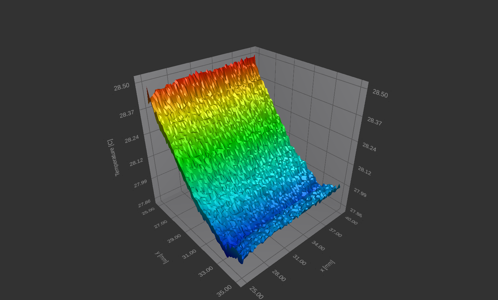
- Temperature influence on the Work Function,
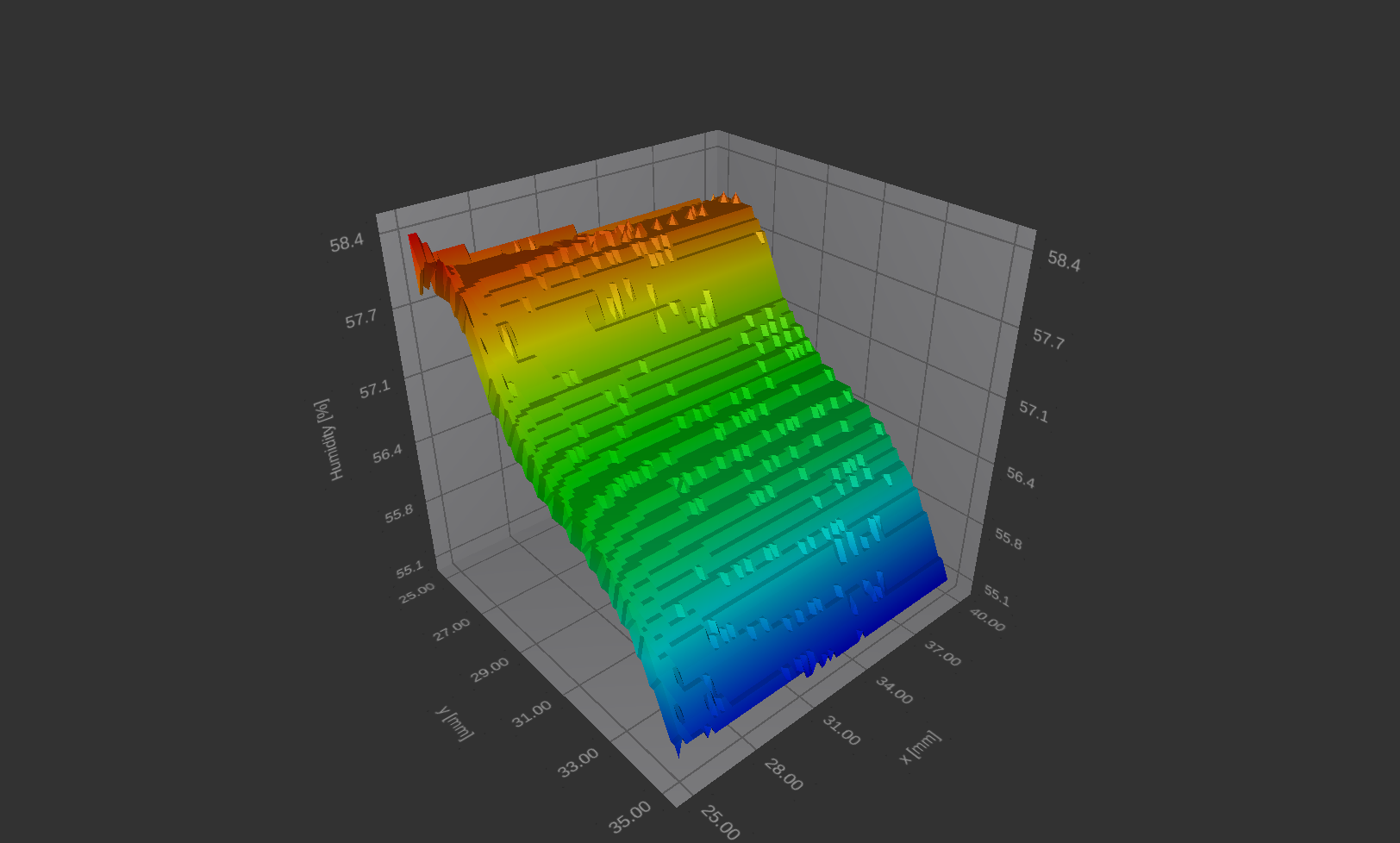
- Humidity influence on the Work Function,
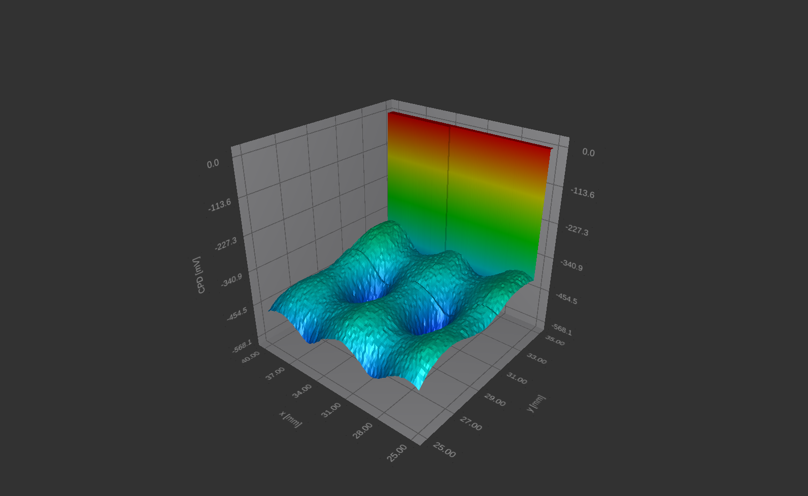
- Electrostatic charge distribution over the surface.
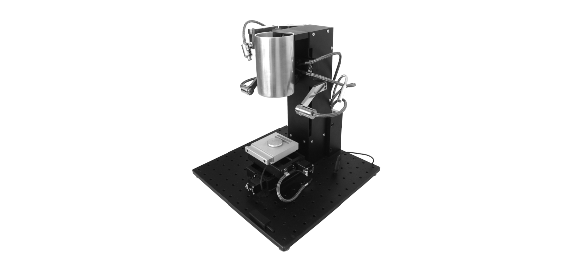
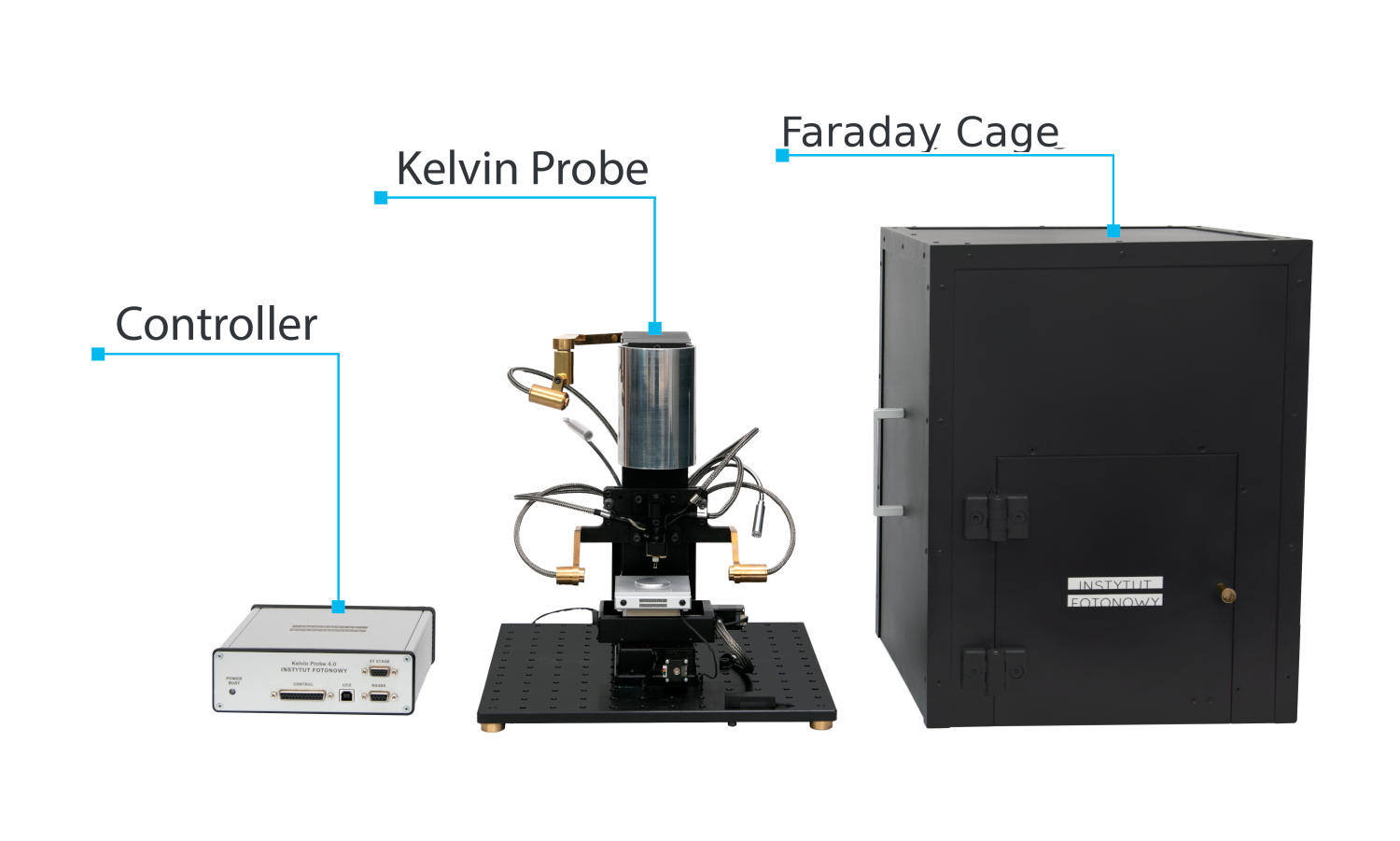
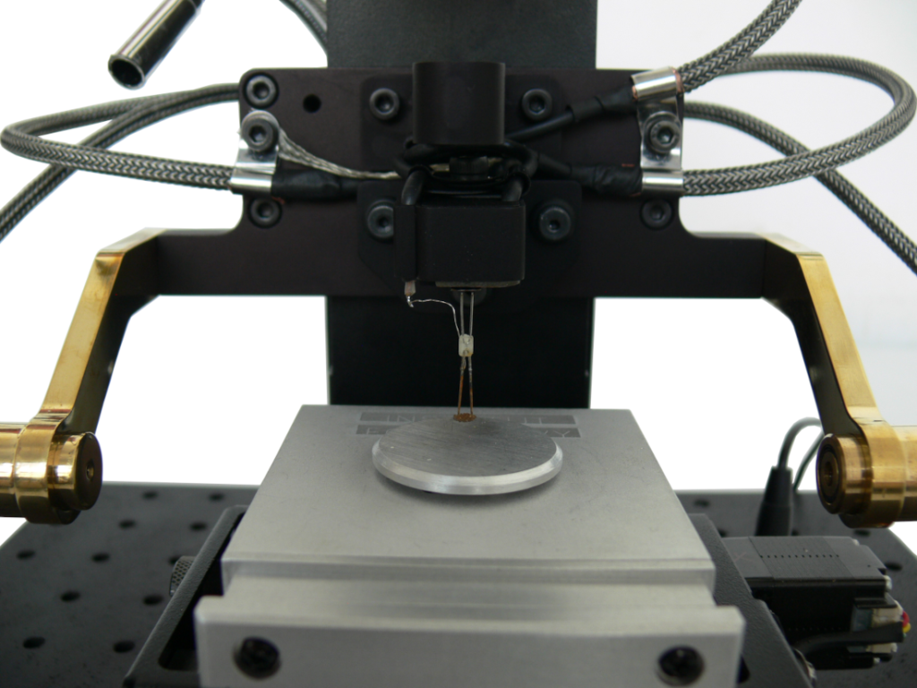
The Kelvin Probe set consists of:
- Controller unit,
- Kelvin Probe instrument with the Probe Tip,
- Faraday Cage.
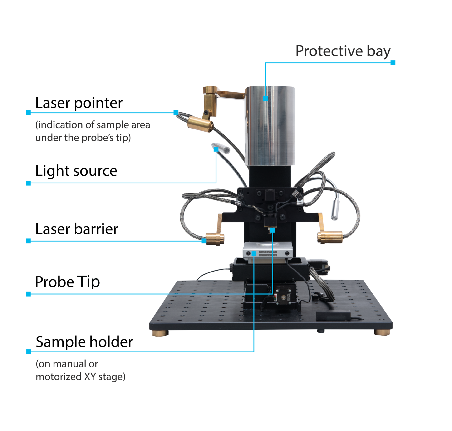
The Kelvin Probe instrument is equipped with:
- Protective bay to park the Probe Tip after experiment,
- Laser pointer to indicate the area directly,
- Light source that helps to handle the sample when the instrument is covered with the Faraday Cage,
- Laser barrier to precisely detect the Probe Tip distance to the sample,
- Golden Probe Tip,
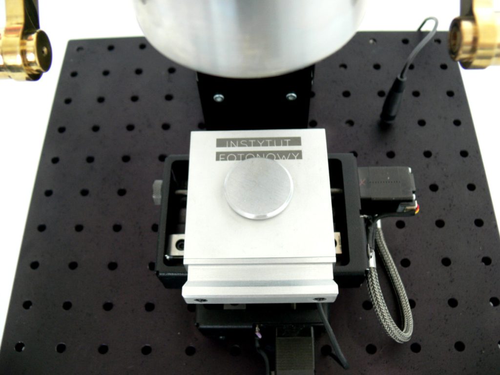
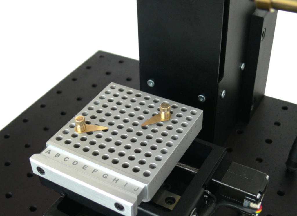
- Sample holder,
- Motorized XY Table.
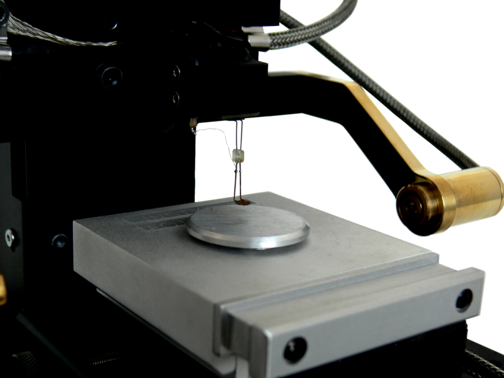
Probe Tip
The most important part of the Kelvin Probe instrument is the Probe Tip. The reference electrode is made of Au mesh of 2.5 mm diameter. It provides high signal to noise ratio, even from a distance of 0.5 mm above the sample. Thus, it does not matter if the examined sample surface is rough or polished. The tip oscillations are generated with an electromagnet.
The Probe Tip is the component fully designed and manufactured by Instytut Fotonowy Sp. z o.o.
click the picture to enlarge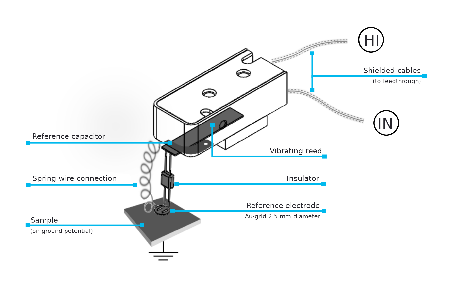
Sample holders
The standard Kelvin Probe Set includes two types of sample stands:
- Bottom contact stand for samples on conducting substrates,
- Top contact stand for non-conducting substrates,
Faraday Cage
The entire instrument is covered with the Faraday Cage, shielding the setup from the ambient light and electromagentic fields.
click the picture to enlarge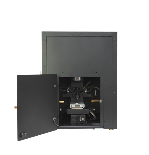
Gas-tight Faraday Cage with inert gas flow system
Scince measurements of the CPD is often sensitive to environmental factors like temperature, humidity, dust and chemical contaminants, Kelvin Probe may be placed inside the hermetic version of the Faraday Cage with the inert gas flow system.
click the picture to enlarge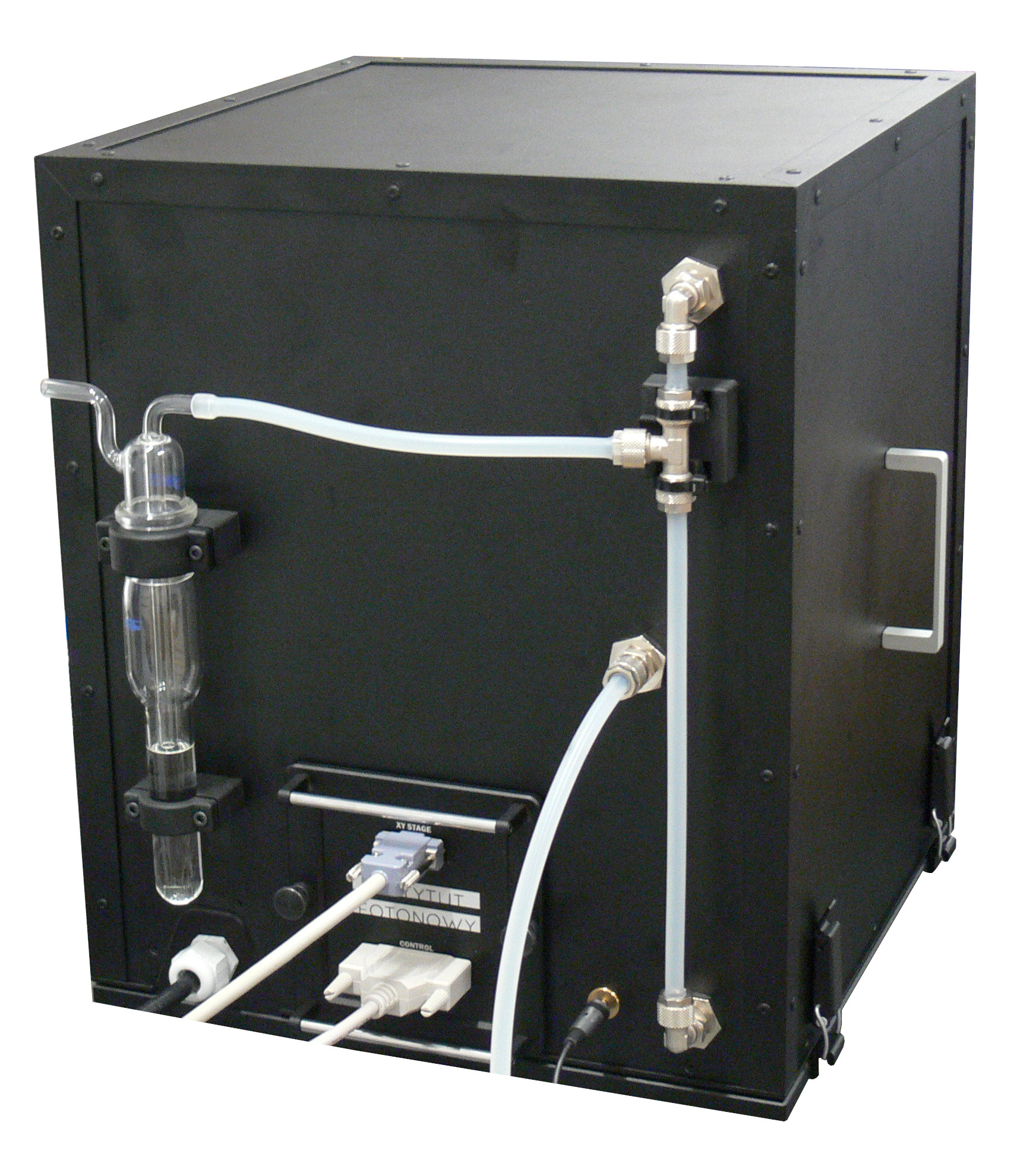
Laser barrier
The Kelvin Probe is equipped with the Laser barrier system. System automatically detects the sample sub-
strate. Each time the probe approaches the sample being examined, an accurate distance between the sample surface and the Probe Tip is measured with 20 µm precision.
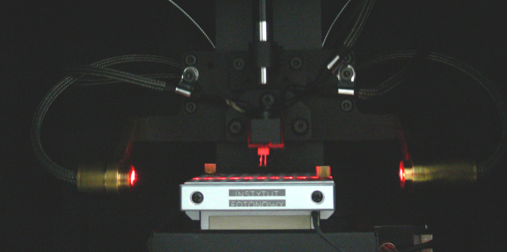
Sample illumination
The sample may be illuminated during the measurements from the optical fiber situated above the Probe Tip. The Probe Tip lets the light through. The light at optical fiber input may be provided by the LED Revolver, Xenon Lamp combined with the Monochromator or any other type of the light source desired.
click the picture to enlarge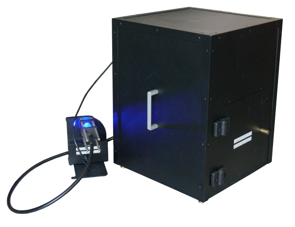
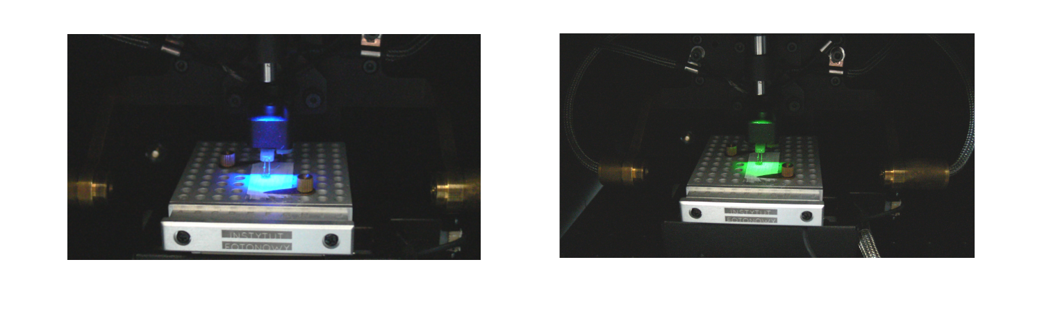
Several types of liquid lightguides from Lumatec may be used to provide the sample illumination.
General:
- Weight: 10 kg,
- Size: 40x40x45 cm,
- PC connectivity: USB 2.0,
- Power supply: 230 V, 50 Hz or 115 V, 60 Hz,
- Measurement technique: 2-channel lock-in-amplifier,
- Laser barrier to automatically detect the substrate and prevent the tip from running into the sample,
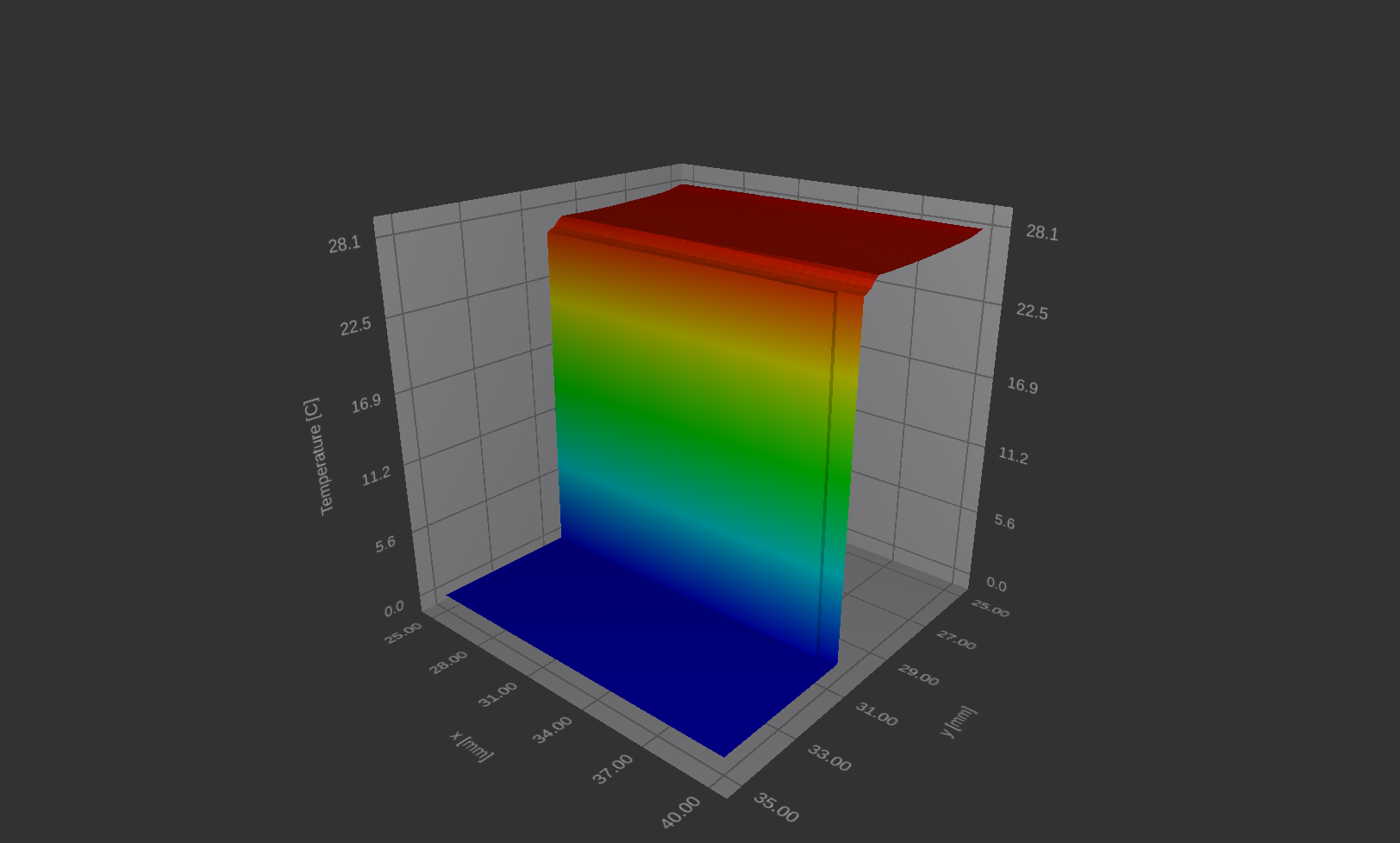
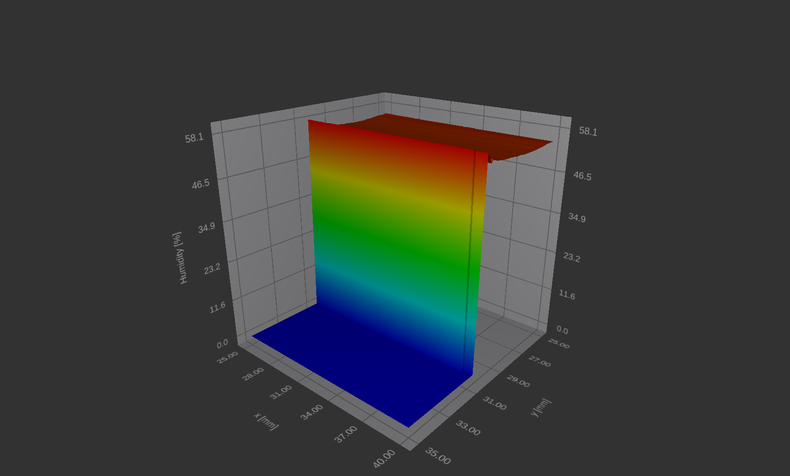
- Auxiliary sensors: humidity, temperature,
- Small lamp,
- Laser pointer for examined point of the surface indication,
- Sample holders:
– Freely shaped solid state with top contact holder,
– Bottom contact holder,
– Electrochemical holder,
Faraday Cage:
- Standard / gas-tight with inert gas flow system,
Measurement unit:
- Bias voltage range: -5 ÷ 5 V,
- Voltage measurement resolution: 0.15 mV,
- Current ranges: 300 nA, 30 nA, 3 nA, 300 pA,
Probe Tip:
- Probe Tip type: Au mesh, 2.5 mm in diameter,
- Tip positioning resolution in vertical axis: 20 µm,
- Automated resonance frequency scanning,
- Adjustable oscillation amplitude,
- Automated removal of the parasitic current of the tip,
- Partial transparency for the light,
- Typical CPD measurement distance: 0.2 – 1 mm,
XY Table:
- Motorized, controlled via software,
- Size: 50 x 50 mm,
- Movement range: 50 x 50 mm,
Aluminium surface
Metal surface sample with periodic holes
Preview during ongoing measurement
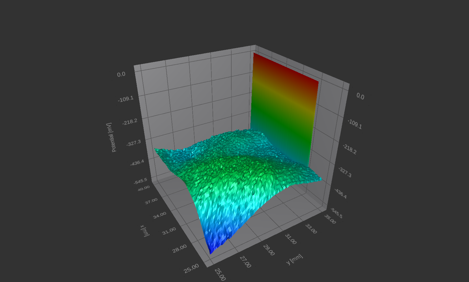
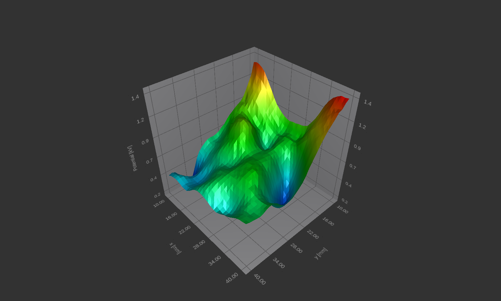
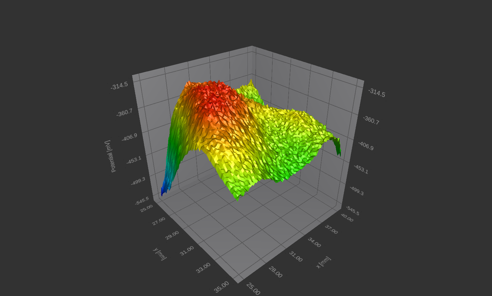
Charge distribution on the dielectric surface
PTFE on alluminium foil – Electric potential from the surface charge of the sample
click the picture to enlarge