扫描开尔文探头 研究样品的电表面状态

专用于测量半导体样品表面的电子功函数。

menu nawigacyjne
0 z 0
描述

扫描开尔文探头可以测量 CPD(接触电位差)值,评估半导体和导电材料的功函数。测量不仅可以在样品表面的单点进行,还可以对整个表面进行扫描。

功函数测量在半导体物理学中特别有用,因为它提供了被测材料费米级的位置。

配备光源的开尔文探针可以检测样品的电子表面状态。电子的表面状态在电荷转移中起着重要作用,这对光伏材料和光电化学尤其重要。

通过扫描样品表面并检查其电学特性,可以精确评估材料的质量及其均匀性。 实验过程中收集的一系列数据可用于更精确地评估工作功能。


静电电压表

扫描式开尔文探头可确定被测样品表面(包括电介质)的静电荷分布!(最高可达几 kV)。该仪器采用的测量方法和设计使其在测试带电介质表面方面独一无二、无与伦比。该系统能够确定样品表面的静电荷分布(最高可达数 kV!)。
 

开尔文探头模块

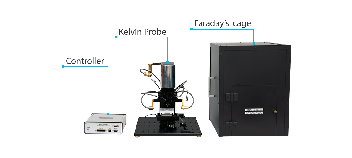
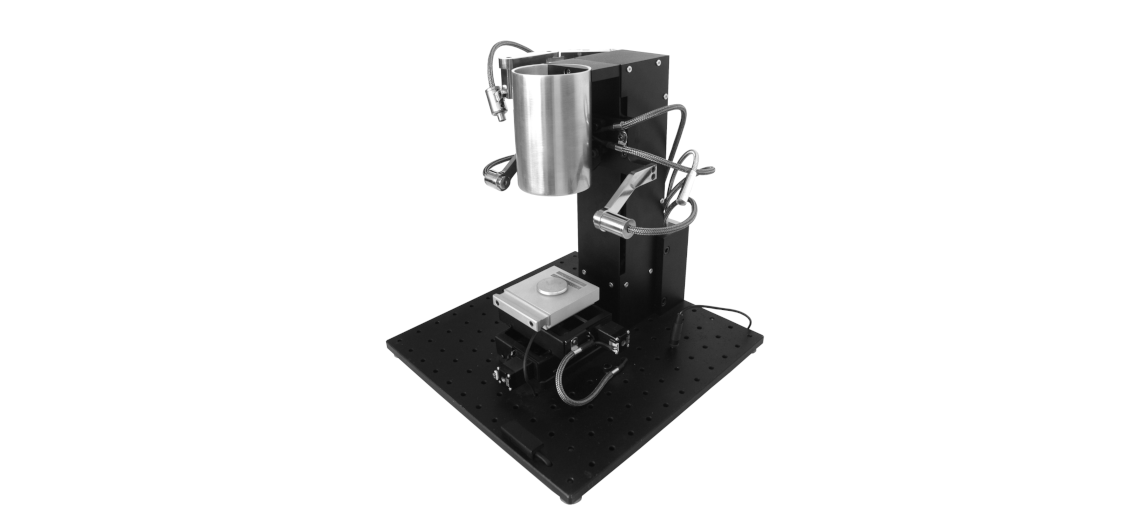
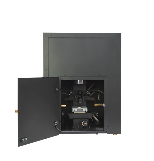
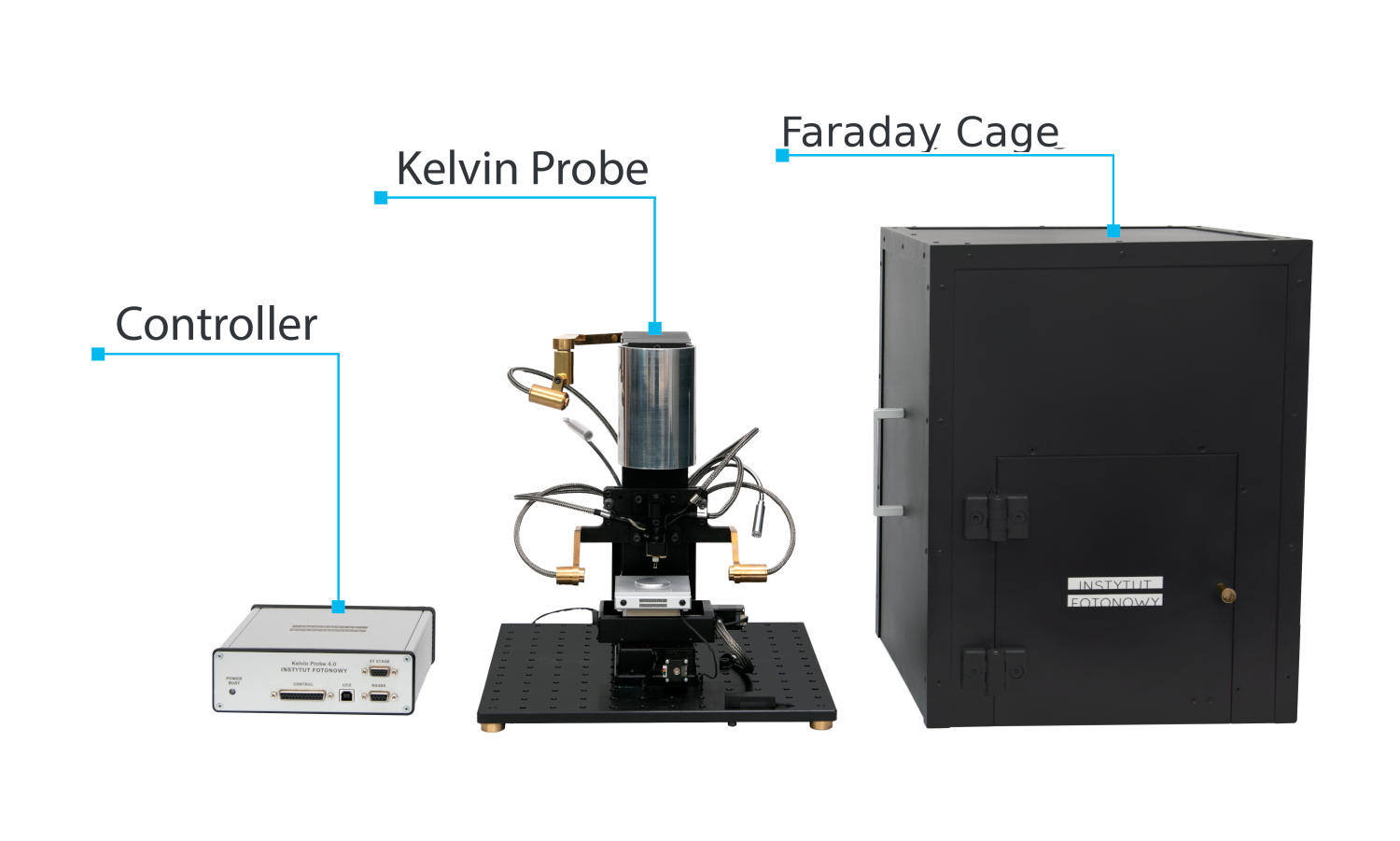
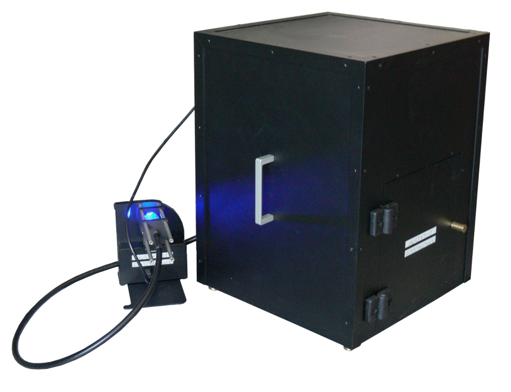
仪器由支架上的探头、电子控制系统和法拉第笼组成。

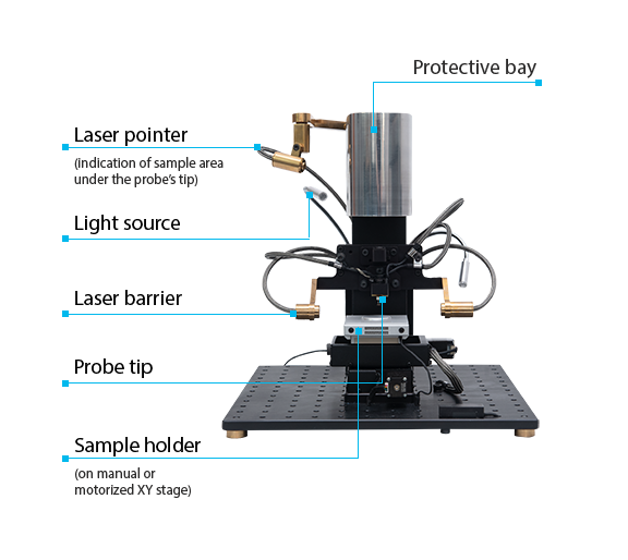
  • 样品放置在 XY 工作台上的两个支架中的一个上。电动工作台可使样品在 X 和 Y 两个方向上移动 5 厘米: X 和 Y 方向移动 5 厘米。
  • 每次探针接近被测样品时,都会精确测量样品表面与探针之间的距离,精度为 50 微米。在所采用的方法中,垂直轴的精度对于确定工作函数并不重要。
  • 探头配有激光指示器,可在测量时照亮探头上方的一个点。光源有助于观察法拉第笼下的样品。
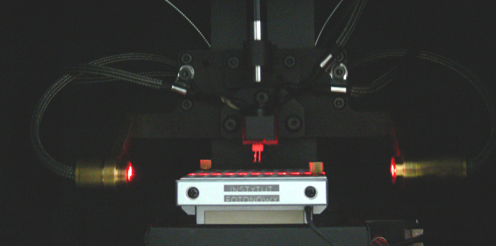
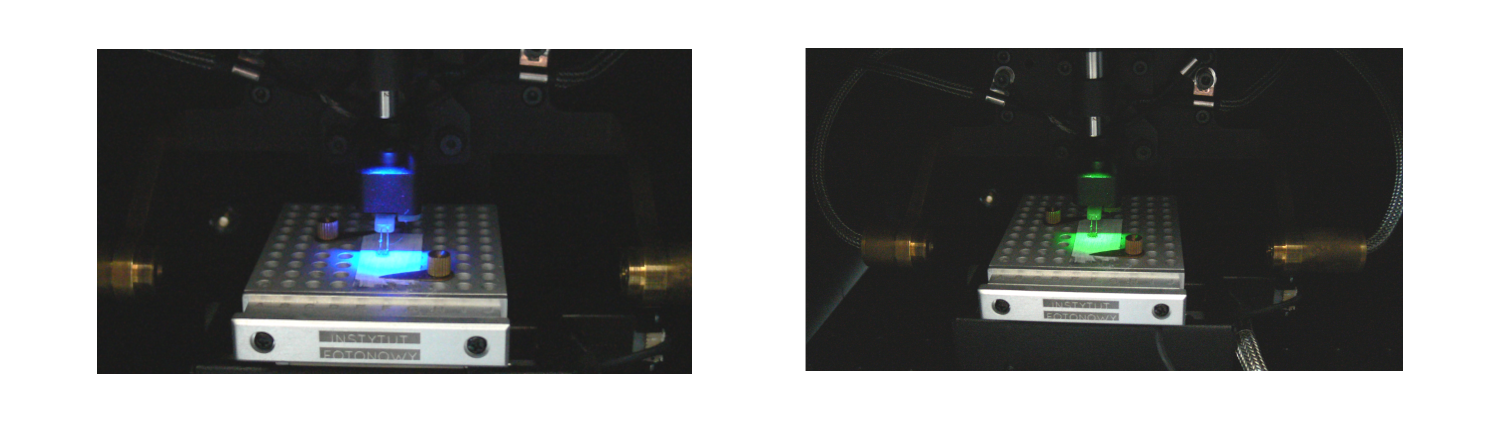
  • 探头上方安装有光纤适配器。光纤可以用单色仪或 LED 左轮手枪发出的光照射样品。
  • 在样品处理过程中,探针隐藏在金属盖下,可防止探针意外损坏。


点击图片放大


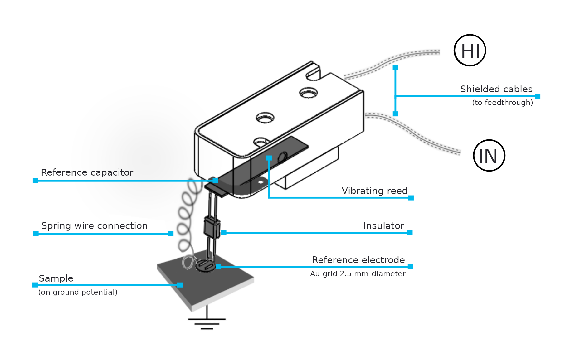
探头尖端

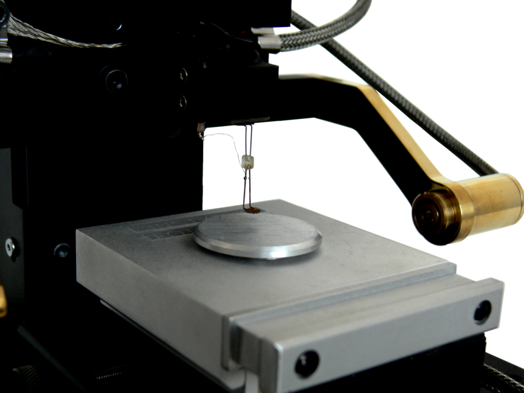
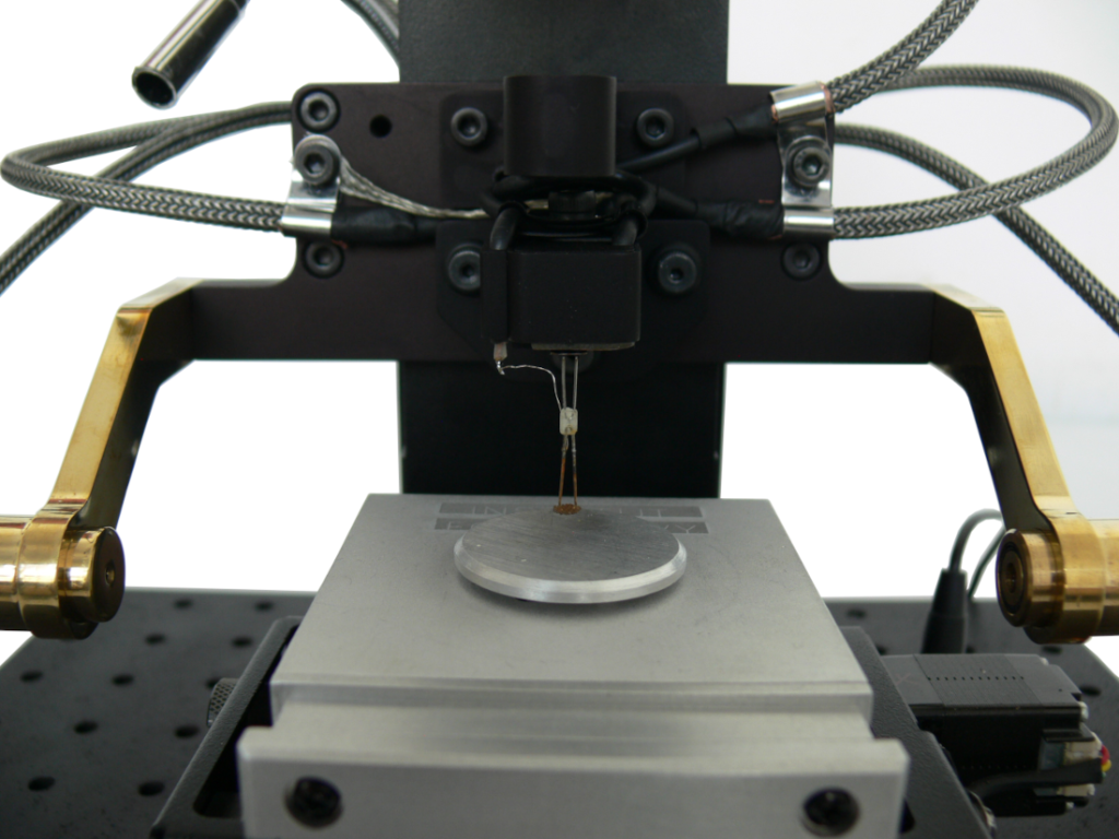
探头尖端是完全由 Instytut Fotonowy 设计和制造的组件,它提供


  • 即使距离样品上方 0.5 毫米,也能发出较大信号。 因此,样品表面是粗糙的还是抛光的并不重要。
  • 让光线透过的透明度。 这样样品就可以被垂直光束照亮。

尖端振荡由电磁铁产生。


点击图片放大

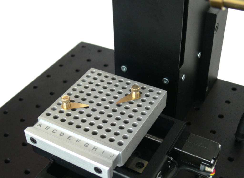
样本持有者

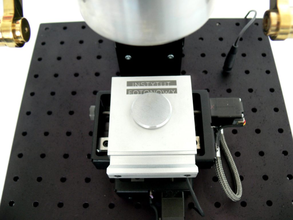
开尔文探针套件包括两种类型的样品台

  • 用于薄膜样品

  • 用于自由成型的固态样品

法拉第笼

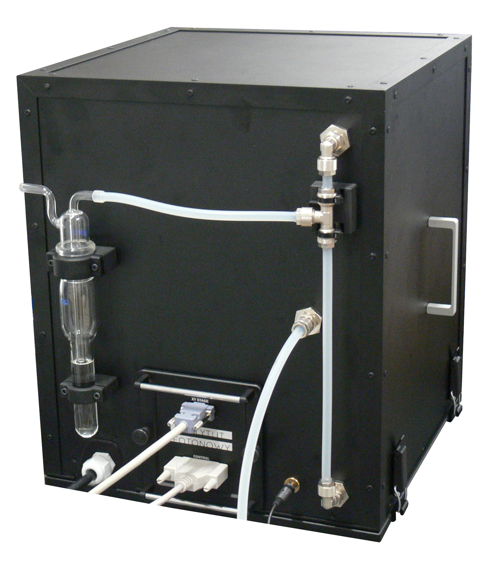
整个测量仪器由法拉第笼罩,使系统与周围环境隔绝。接地插座位于法拉第笼上。

点击图片放大


规格


根据设备开发的进一步进程,以下规格可能会有所改变。


Voltage range-5 V .. 5 V
Voltage measurement nominal resolution0.15 mV
Measurement technology2-channel lock-in amplifier
Sample holdermotorized translation stage X-Y,
Sample standstand for sample layer/ stand for solid state sample
Range of stage movement5 cm x 5 cm
Min sample move step1 µm
Tip typeAu, mesh, dia. 2.5 mm
Tip Z positioningmotorized Z stage
Positioning with respect to a samplelight barrier
Tip Z positioning resolution10 µm
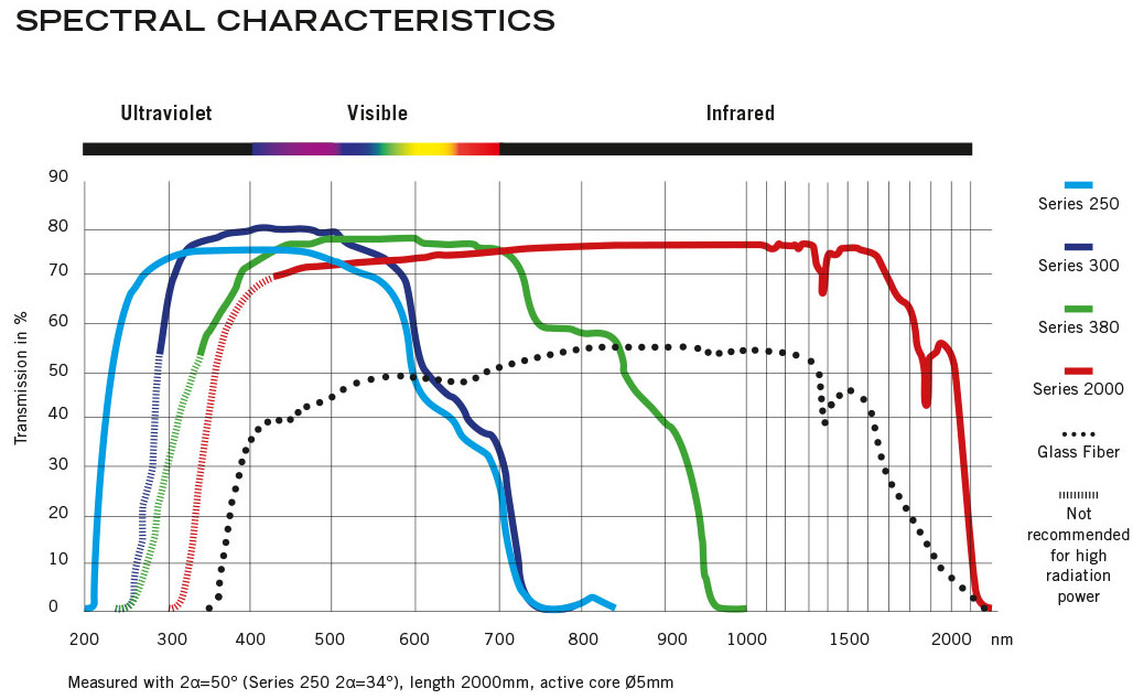
Spectral range for wave guides200 nm .. 2000 nm (depending on a waveguide)
Liquid waveguides selection (Lumatec)Wybór światłowodów Lumatec
Auxiliary sensorshumidity and temperature
Internal Faraday cage illuminationwhite LED
X-Y positioning aidlaser sample placement indicator
PC connectivityUSB 2.0
Size40 x 40 x 45 cm
Weight15 kg

典范成果

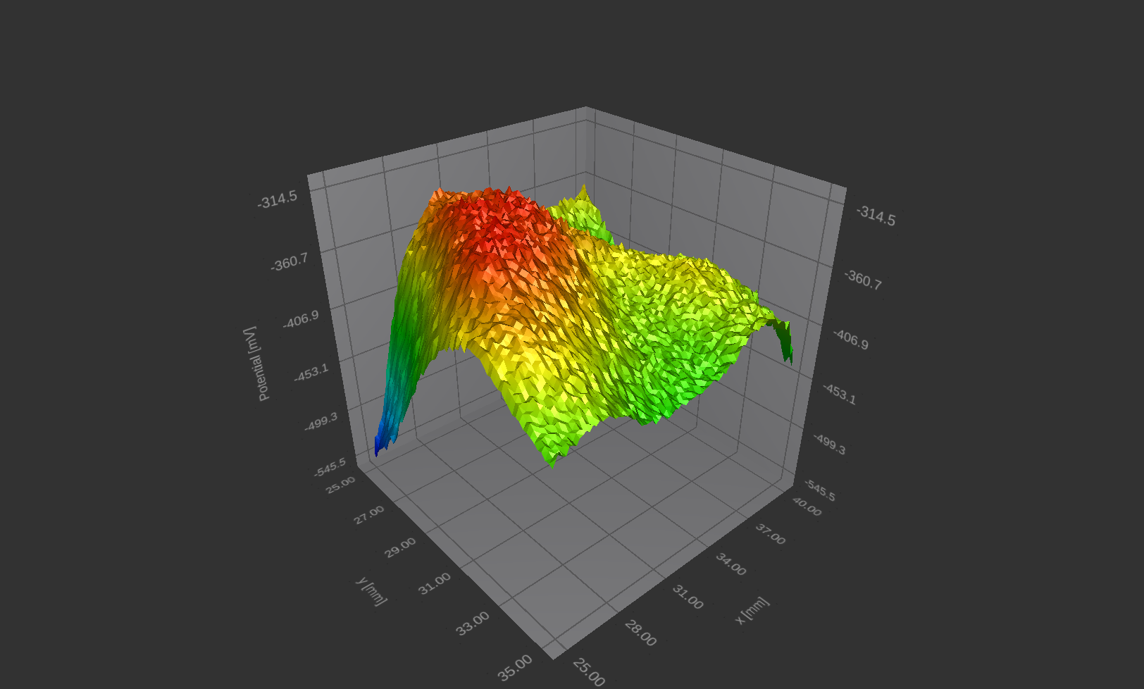
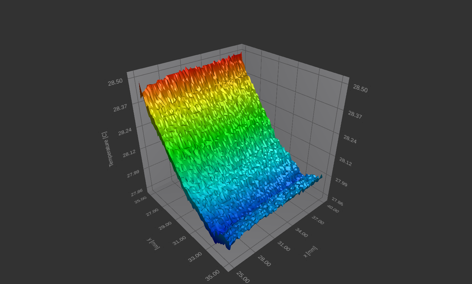
铝表面

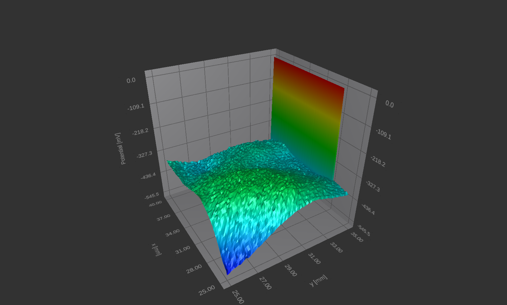
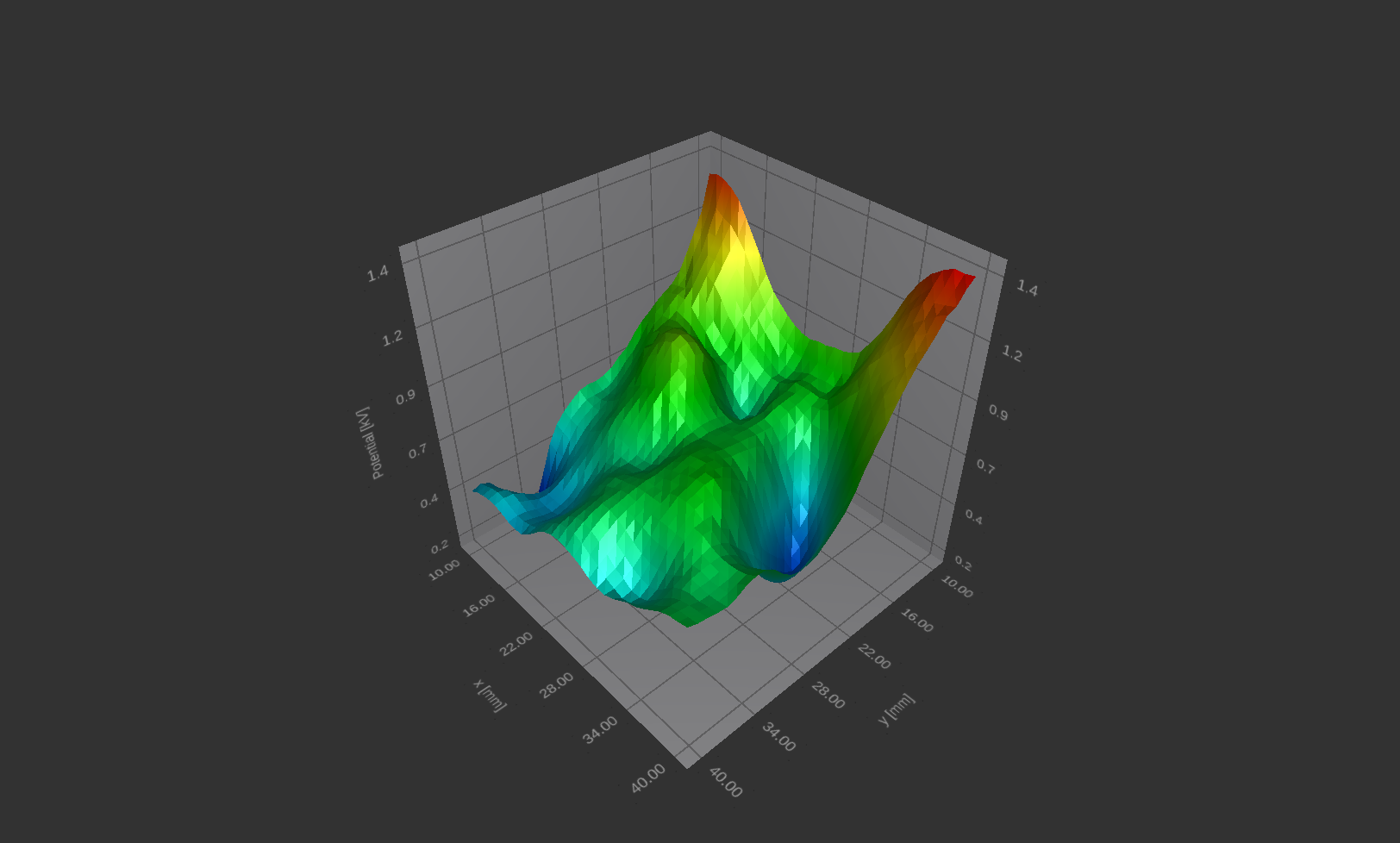
样品表面的电动势分布

点击图片放大

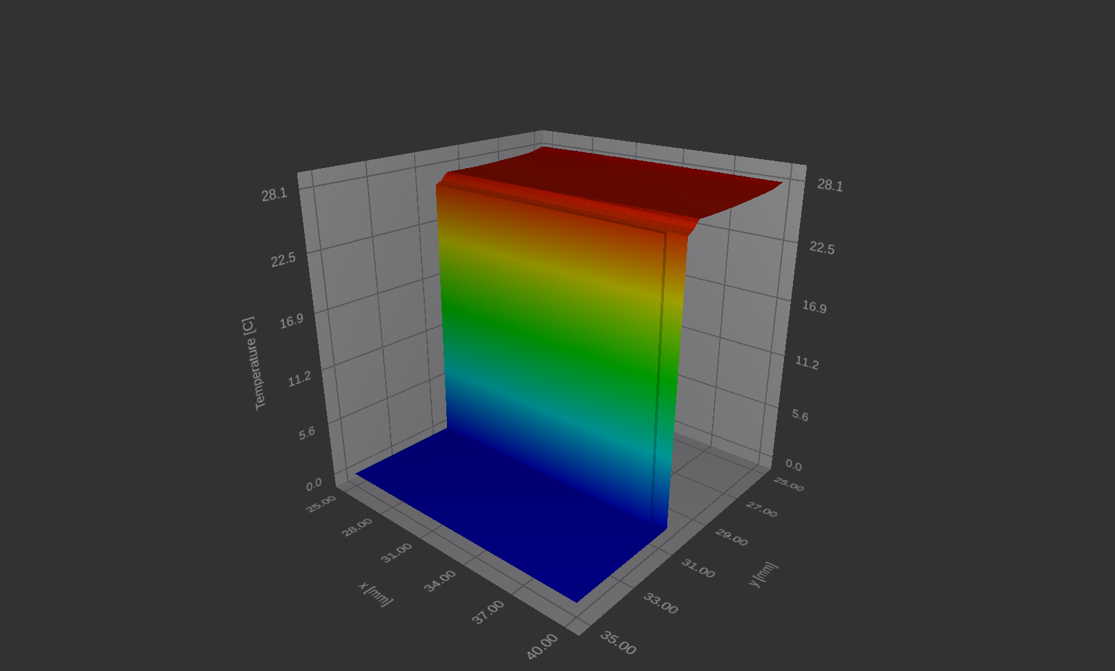
测量时的环境温度

点击图片放大

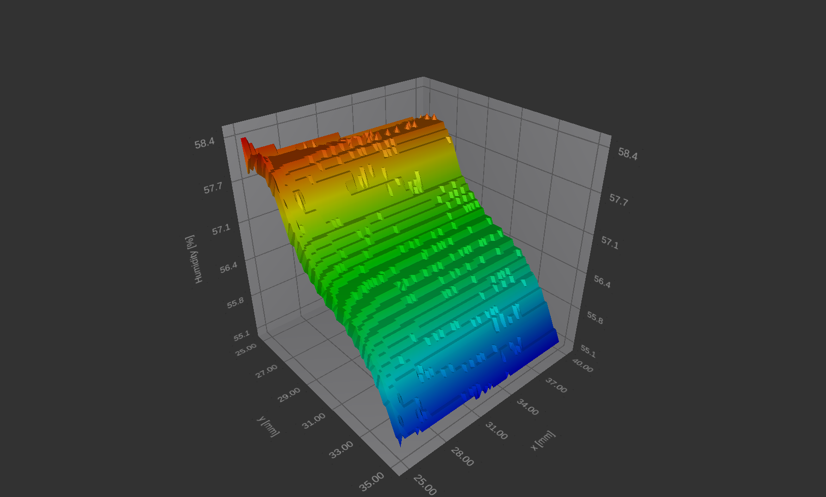
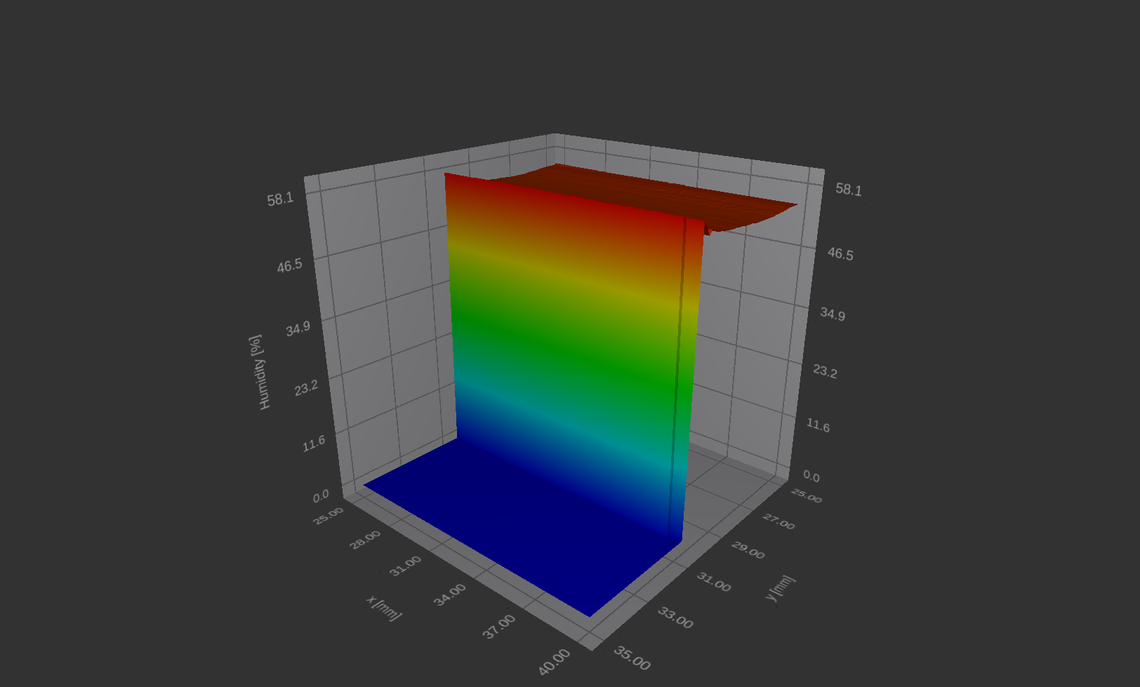
测量过程中的空气湿度

点击图片放大

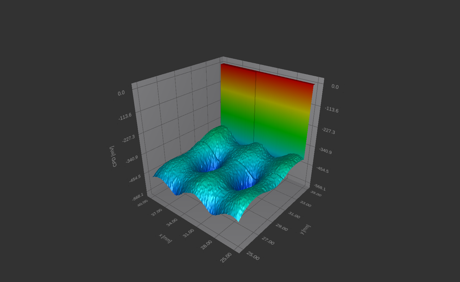
带周期性小孔的金属表面样品

表面 CPD 评估值

点击图片放大

测量过程中的预览

样品表面的电动势分布

点击图片放大

测量过程中的环境温度

点击图片放大

测量过程中的空气湿度

点击图片放大

介质表面的电荷分布

铝箔上的聚四氟乙烯 – 来自样品表面电荷的电动势

点击图片放大

SKONTAKTUJ SIĘ Z NAMI
ZOSTAW KONTAKT DO SIEBIE - Odezwiemy się w przeciągu 48h


    I agree that provided personal information will be processed by Instytut Fotonowy Sp. z o.o. only for the purpose of business offer for the relevant product.

    SKONTAKTUJ SIĘ Z NAMI - Odpowiemy na wszystkie Twoje pytania. + 48 733 003 380 office@fotonowy.pl

    Podobne produkty

    Scanning Kelvin Probe to investigate surface states of the sample

    Dedicated to measure Contact Potential Difference and charge distribution over the sample surface.

    Description

    Scanning Kelvin Probe allows to measure the Contact Potential Difference (CPD) not only in a single point of the sample but the entire sample surface may be scanned.
    Kelvin Probe equipped with a light source enables to examine surface states of electrons in the sample. Surface states of electrons play a significant role in electric charge transfer, which is especially important for photovoltaic materials and in photoelectrochemistry.
    Possibility of scanning the sample surface and to examine its electrical properties enables precise assessment of the quality of the material, its homogeneity, etc. The series of CPD values collected for many points of the sample, may be used to evaluate Work Function more precisely.

    Electrostatic Voltmeter

    The measurement technique, analytic methods applied and the design of the instrument makes the instrument unique and peerless in testing charged dielectric surfaces, including dielectrics where the measured potential above the accumulated charges may be as large as several kilovolts!

    Scanning Kelvin Probe system enables to investigate:

    • The Work Function of a material,
    • Position of Fermi level with respect to the conduction and valence band edges,
    • The type, n or p, of a semiconductor,
    • Energy gap of a semiconductor,
    • Surface potential (SPV by flat band technique),
    • Surface adsorption and chemisorption effects on the Work Function,
    • Information on the surface states density,
    • Surface charging and discharging effects,
    • Minority carriers diffusion length,
    • Carrier recombination rates (especially for indirect bandgap semiconductors),
    • Information on buried interfaces,
    • Temperature influence on the Work Function,
    • Humidity influence on the Work Function,
    • Electrostatic charge distribution over the surface.


    kelvin probe modules

    The Kelvin Probe set consists of:

    • Controller unit,
    • Kelvin Probe instrument with the Probe Tip,
    • Faraday Cage.
    click the picture to enlarge

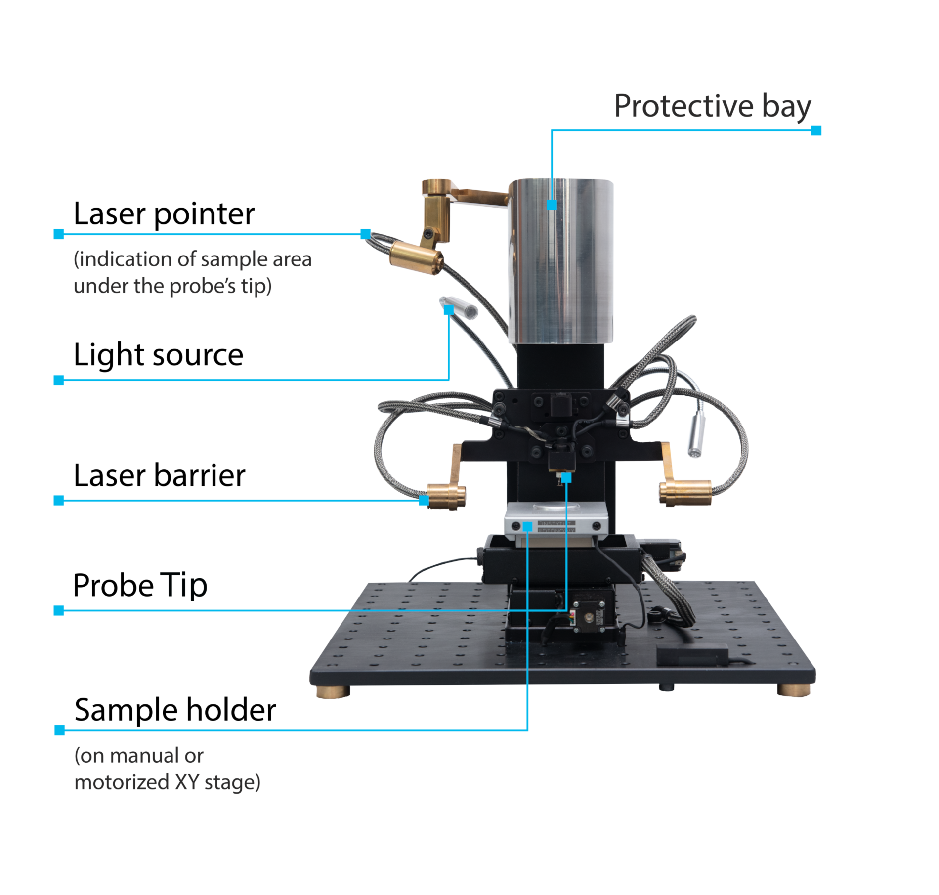
    The Kelvin Probe instrument is equipped with:

    • Protective bay to park the Probe Tip after experiment,
    • Laser pointer to indicate the area directly,
    • Light source that helps to handle the sample when the instrument is covered with the Faraday Cage,
    • Laser barrier to precisely detect the Probe Tip distance to the sample,
    • Golden Probe Tip,
    • Sample holder,
    • Motorized XY Table.
    click the picture to enlarge

    Probe Tip

    The most important part of the Kelvin Probe instrument is the Probe Tip.  The reference electrode is made of Au mesh of 2.5 mm diameter. It provides high signal to noise ratio, even from a distance of 0.5 mm above the sample. Thus, it does not matter if the examined sample surface is rough or polished. The tip oscillations are generated with an electromagnet.

    The Probe Tip is the component fully designed and manufactured by Instytut Fotonowy Sp. z o.o.

    click the picture to enlarge


    Sample holders

    The standard Kelvin Probe Set includes two types of sample stands:

    • Bottom contact stand for samples on conducting substrates,

    • Top contact stand for non-conducting substrates,

    Faraday Cage

    The entire instrument is covered with the Faraday Cage, shielding the setup from the ambient light and electromagentic fields.

    click the picture to enlarge

    Gas-tight Faraday Cage with inert gas flow system

    Scince measurements of the CPD is often sensitive to environmental factors like temperature, humidity, dust and chemical contaminants, Kelvin Probe may be placed inside the hermetic version of the Faraday Cage with the inert gas flow system.

    click the picture to enlarge

    Laser barrier

    The Kelvin Probe is equipped with the Laser barrier system. System automatically detects the sample sub-
    strate. Each time the probe approaches the sample being examined, an accurate distance between the sample surface and the Probe Tip is measured with 20 µm precision.

    click the picture to enlarge


    Sample illumination

    The sample may be illuminated during the measurements from the optical fiber situated above the Probe Tip. The Probe Tip lets the light through. The light at optical fiber input may be provided by the LED Revolver, Xenon Lamp combined with the Monochromator or any other type of the light source desired.

    click the picture to enlarge
    Several types of liquid lightguides from Lumatec may be used to provide the sample illumination.

    Lumatec wave guides types

    Specifications

    General:

    • Weight: 10 kg,
    • Size: 40x40x45 cm,
    • PC connectivity: USB 2.0,
    • Power supply: 230 V, 50 Hz or 115 V, 60 Hz,
    • Measurement technique: 2-channel lock-in-amplifier,
    • Laser barrier to automatically detect the substrate and prevent the tip from running into the sample,
    • Auxiliary sensors: humidity, temperature,
    • Small lamp,
    • Laser pointer for examined point of the surface indication,
    • Sample holders:
      – Freely shaped solid state with top contact holder,
      – Bottom contact holder,
      – Electrochemical holder,

    Faraday Cage:

    • Standard / gas-tight with inert gas flow system,

    Measurement unit:

    • Bias voltage range: -5 ÷ 5 V,
    • Voltage measurement resolution: 0.15 mV,
    • Current ranges: 300 nA, 30 nA, 3 nA, 300 pA,

    Probe Tip:

    • Probe Tip type: Au mesh, 2.5 mm in diameter,
    • Tip positioning resolution in vertical axis: 20 µm,
    • Automated resonance frequency scanning,
    • Adjustable oscillation amplitude,
    • Automated removal of the parasitic current of the tip,
    • Partial transparency for the light,
    • Typical CPD measurement distance: 0.2 – 1 mm,

    XY Table:

    • Motorized, controlled via software,
    • Size: 50 x 50 mm,
    • Movement range: 50 x 50 mm,


    Exemplary results

    Aluminium surface

    Distribution of the electric potential on the sample surface:

    click the picture to enlarge

    Ambient temperature during measurement:

    click the picture to enlarge

    Air humidity during measurement:

    click the picture to enlarge

    Metal surface sample with periodic holes

    Evaluated CPD values on surface:

    click the picture to enlarge

    Preview during ongoing measurement

    Distribution of the electric potential on the sample surface:

    click the picture to enlarge

    Ambient temperature during ongoing measurement:

    click the picture to enlarge

    Air humidity during ongoing measurement:

    click the picture to enlarge

    Charge distribution on the dielectric surface

    PTFE on alluminium foil – Electric potential from the surface charge of the sample

    click the picture to enlarge

    SKONTAKTUJ SIĘ Z NAMI
    ZOSTAW KONTAKT DO SIEBIE - Odezwiemy się w przeciągu 48h


      I agree that provided personal information will be processed by Instytut Fotonowy Sp. z o.o. only for the purpose of business offer for the relevant product.

      SKONTAKTUJ SIĘ Z NAMI - Odpowiemy na wszystkie Twoje pytania. + 48 733 003 380 office@fotonowy.pl

      Podobne produkty

      71703.40364.1696